About transistors - Part 8 : FETs
Let's talk about JFETs and MOSFETs !
Let's talk about JFETs and MOSFETs !
Today's topic concerns FETs.
FETs are Field-Effect Transistors, and there are many types of them, but I will only focus on JFETs and MOSFETs, which are the most used in audio. FETs all use the same physics : instead of using P and N junctions in the same way as BJTs, we block or pass the current using an electric field which is modulated by a voltage. I will explain how JFETs and MOSFETs work internally in comparison with bipolar transistors. The current versus voltage equation is the same for both however, and the calculation are the same in circuits for these transistors as for bipolar transistors. Drain is somewhat equivalent to the collector, source is equivalent to the emitter and gate is equivalent to the base of a bipolar transistor.
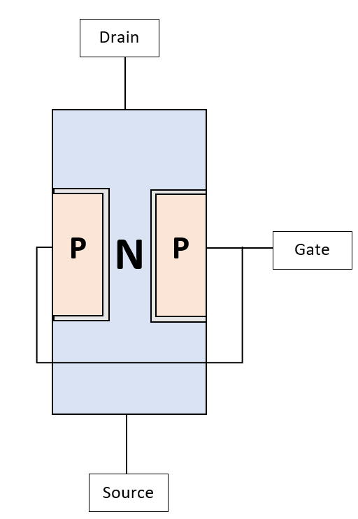
Let's talk about Junction FET, or JFETs first. A JFET is based on a single PN junction, exactly like a diode in fact ! A N-channel JFET is made of a large N junction with two P junctions around it. Applying a voltage on this junction will neutralize the gap from one end of the N junction to the other, effectively reducing the space for the electrons to flow. Of course, a voltage of the opposite sign will allow more electrons to flow, widening the gap. The neutralized region which does not conduct electrons is called the depletion region. The P junctions are tied together and called the grid, and the ends of the N junction are called drain and source. The difference between them is the amount of doping at each end. The depletion region is colored in grey on the picture. You guessed it, because it has a P junction connected to a N junction, the JFET has an intrinsic diode that can NEVER be reverse-biased without burning the transistor ! This means the source must always stay more positive than the gate by a diode drop Vd, which is not usual if you remember bipolar transistors. Actually, it can remind you of how a tube work, because a tube will leak current through its grid if its cathode is not biased high enough compared to the grid !
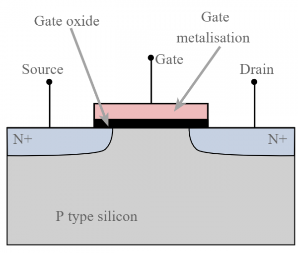
MOSFETs work a bit the same way, but instead of a PN junction with a depletion region controlling the gap, it works with a metal gate insulated from the channel by an oxide. Hence the name Metal Oxide Semiconductor FET. The voltage applied on the gate has exactly the same effect as with the JFET and controls the current flowing from drain to source. Electronic-notes.com has a wonderful diagram to represent a MOSFET. Not shown on the diagram, the subtrate where all these semiconductors lay, which is called the body, must always be connected to the most negative potential of the transistor. Usually it is connected to the source, but it is sometimes left open for the engineer to solder it to another potential. By doing so, the substrate forms a diode, called the body diode, which is a flaw of the transistor but necessary for operation unfortunately.
Both of these components have the same I-V curves. The current Id flowing through the device is controlled by the gate-source voltage Vgs following the equation : Id = 0.5*K*Cox*µox*(W/L)*(Vgs - Vp)². Ok, it looks complicated and only applies to MOSFETs, but all the parameters K, Cox, µox, W, L and Vp refer to constant parameters depending on the geometry, doping, etc... An easier and equivalent equation is Id = Idss*(Vgs/Vp - 1)² which is also compatible with JFET this time. This square law gives different saturation characteristics compared to bipolar transistors or diodes.
Vp may be the most important parameter of this equation : it is the pinch voltage. At this voltage, no current can flow in the transistor anymore, both for a JFET or a MOSFET. JFETs always have a more or less wide depletion region, hence they are conducting even when source and gate are at the same potential. Hence, Vp is always negative. In a MOSFET, no destruction can occur in the PN junction because of wrong biasing, and Vp can also be positive. In this case, MOSFET are said to be in enhancement mode. When Vp is negative, the MOSFET is in depletion mode. Very few P channel MOSFETs in depletion mode were designed, and most depletion mode MOSFET are N channel only. To sum this up, depletion mode conduct even when Vgs = 0 and Vp is negative. For enhancement mode, Vp is positive and the transistor doesn not conduct when Vgs = 0.
The true advantage of FETs are their input impedance : it is infinite at DC, meaning no biasing current will flow at all in the gate of these transistors ! The gate-source junction of JFETs work like a reverse diode and like a capacitor for a MOSFET. It means the only gate power dissipated by these transistors comes from the commutation and not the biasing itself. When it comes to the fundamental or more complex circuits, you can simply use JFETs and MOSFETs with their equation and it will also work the same way ! Noise is higher in JFETs than in bipolar, and even more in MOSFETs, but they can easily handle way more power and various power MOSFETs are used to design power amplifiers.
Let's sum this up ! Input impedance of FETs is infinitely higher than for BJTs and their square Id = f(Vgs) law just work a bit differently than the exponential law of the BJT transistor. Apart from that you can also build current mirrors, differential pairs, and opamps from FETs, and they work flawlessly with just different characteristics than BJTs !