About transistors - Part 3 : fundamental circuits
We know how it works, let's use it !
We know how it works, let's use it !
Quick summary ! A transistor is an active component with three poles (emitter, base, collector) arranged so that the voltage Vbe from emitter to base controls the current Ie flowing in the emitter. Usually, the base current is really small compared to the collector current, and is often neglected in calculations.
In today's tutorial, I'll start using schematics to explain the working of circuits. To understand how things are connected, here are the symbols for both NPN and PNP transistors. You'll often see PNP transistors reversed in some schematics, which make them difficult to analyze at first ! Remember the emitter is always the branch with the arrow. You'll also find a lot of different symbols describing the same component, but they're usually easy to recognize.
![]()
Because the equation followed by the transistors is a bit hard to use in most case, techniques and models have been developped which simplify the circuit design process. When analyzing a circuit, the guideline is as follow : first identify the structures used, then analyze their biasing and finally their small-signal behaviour.
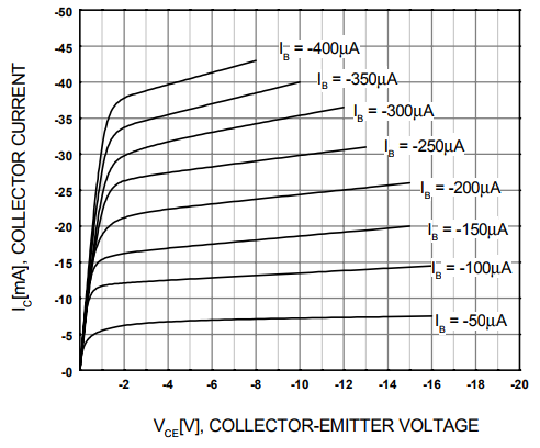
Biasing a transistor is simply powering it, giving it the necessary DC voltage and current to make it work as intended in the circuit. In fact, that's exactly the same for vacuum tubes, and it's not black magic either ! A transistor can operate in three regions depending on Vce and Ib. The first one, not shown in the graph, is the cutoff region, when Vce is made negative or Ib is insufficient. In this region, no current can flow in the transistor - or so little that it's negligible. When Vce is made higher, between 0V and the voltage drop of the PN junction, Vd, the transistor behaves almost like a resistor. Ic is roughly proportionnal with Vce, and it is called the saturation region. When Vce is higher than Vd, the transistor stays in its active region. In this case, we can use it for amplification, filtering, etc... This is the "normal" region used in guitar effects.
This is only part of the biasing of a transistor, because it doesn't account for the input signal. In the following circuits, let's say each transistor is correctly biased and that they all operate in the active region. Again, there are three fundamental structures to know when working with transistors. These are building blocks for more complex circuits and can be combined to make preamps or distorsion pedals, for example. Green is for voltage, while red is for current. Each branch of the transistor is either an input, an ouput or common to both, hence the names of common collector, common emitter and common base amplifiers.
%20-%20Sheet1.SchDoc%20_%20-%20Test.PrjPcb.%20Not%20signed%20in..png?1564044196952)
The first structure, on the left, is the common collector, because the collector is neither an input or an output, and it is connected to a voltage reference, VCC. It is the positive pole of the power supply, while ground is the negative one. In this configuration, the emitter is connected to ground through a resistor. When an input voltage is applied to the base of the transistor, the base-emitter PN junction acts like a diode and only drops the base voltage by a constant value Vd. Hence, the ouput voltage is the same as the input voltage minus Vd : Vout = Vin - Vd. With a little bit of math, small-signal equation is obtained by differentiating the previous one : dVout = dVin. This structure is a voltage buffer. The output is the input voltage, but has a lot more current available.
The second structure is the only one able to amplify an input signal. It is called the common emitter amplifier. DC analysis gives us that Vbe is constant and equals Vd, the voltage drop of the base-emitter junction. Hence, we should have Vin = Vd, it should be constant ! The reason we can say Vin still varies is that we consider it as the sum of a "constant" signal and a "negligible", varying signal : Vin = Vin0 + dVin. We will also write that for every other current and voltage. The DC analysis gives us Vin0 = Vd. Small-signal analysis gives us the output current dIe = gm*dVin. The transconductance gm can be calculated by differentiating the Shockley Law and equals Ic0/Vt, where Vt is the thermal voltage and Ic0 is the DC collector current. Wait, you just wrote dIe, which is not really the output, is it ? Indeed, and in order to get dIc, we have to remember that Ic = hfe*Ib hence Ic = Ie*hfe/(hfe+1). We now get dIc = [hfe/(hfe+1)]*gm*dVin which is almost the same formula when hfe is high enough.
The last structure is the common base amplifier. Both input and output are current, and because the base is tied to ground, Ib is constant. Differentiating the equation Ie = Ic + Ib will hence give us dIe = dIc. This time, the structure is a current buffer.
This article has a lot of information in it, don't worry if you don't understand everything in once ! You can always pause and come back later, or switch to another article if you want to see some circuit analysis. Please ask questions in the comment if you have any !