About transistors - Part 4 : models
Let's explore small-signal analysis and impedance.
Let's explore small-signal analysis and impedance.
Welcome back ! Last episode was about fundamental structures, but to understand them fully you need to talk about impedance. So let's crack open a transistor and draw a model for it !
First thing to keep in mind is that a model is a simplified representation of a component and is just a tool for calculations and circuit design. A model shouldn't be taken as a working circuit ! A lot of models exist for transistors, but I'll only talk about two of them : the Ebers-Moll model and Hybrid Pi model.
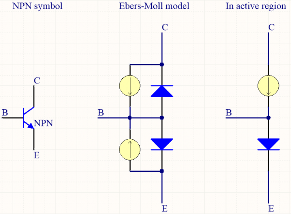
The Ebers-Moll model, also called sometimes T-shaped model, describes the transistor with two current sources and two diodes in parallel. Depending on the operating region of the transistor, diodes pass current or block it and the current sources are active or not. When operating in the active region, there is only one current source and one diode passing current. Now we see why there is a voltage drop Vd between emitter and base, and how the current flows in the transistor ! The current source has an output current of Ic = hfe*Ib.
When talking about small-signals, there is only a very small variation of all the voltages and currents in the transistor. We know that a diode, being a PN-junction, follows the Shockley Law. By differentiating this law at the operating point, we can say that the diode acts like a dynamic resistor, as far as these small-signals are concerned. Then, you can simply replace the diode in the right Eber-Molls model by a resistor with a resistance of rd = dVbe/dIe = Vt/Ic0. Well, remember the last article ? We exactly find that rd = 1/gm, the dynamic resistance of the diode equals the inverse of the transconductance !
This model is useful to understand the most basic operations achieved by a transistor, but isn't always easy to use, especially when calculating input and output impedance of circuits. Impedance is the ratio of the complex numbers representing voltage and current. Hence, the input impedance of a circuit is Zin = dVin/dIin, while the output impedance is Zout = dVout/dIout. For example, let's take our transistor in the Eber-Molls model just above. If we put an input voltage Vin between base and emitter, there will be a current flowing through the base-emitter diode equal to Ie = Ic+Ib. However, we also know that Ic = hfe*Ib, and that Ib = Iin. We can then simply write Ie = (hfe+1)*Iin. We know that Vbe is a function of Ie - Shockley Law ! - but when calculating impedance, we should only talk about small-signal models. Hence dVin = rd*dIe = rd*(hfe+1)*dIin. We now have a circuit with an input impedance of Zin = dVin/dIin = rd*(hfe+1). The transistor seems to boost the dynamic resistance of its base-emitter junction ! When connecting a resistor Re between emitter and ground, we obtain a circuit with a really high input impedance of Zin = (rd+Re)*(hfe+1) - the common collector fundamental structure. There will be an article only talking about impedance stuff, because it is not only used in transistor circuits but everywhere in electronics !
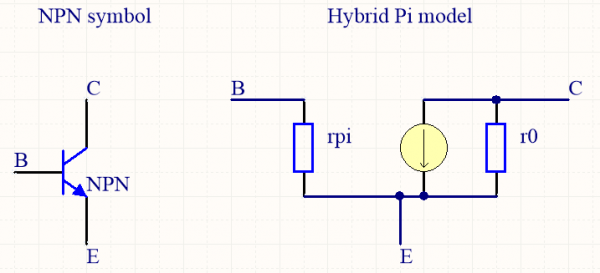
When dealing with impedance, the Hybrid Pi model is easier to use than the Ebers-Moll model. Here, rpi is the input impedance of the transistor, and is equal to rd*(hfe+1). The current source supplies a current Ic = gm*Vbe. However, we haven't talk about r0 yet. This resistance is called the Early resistance, and is the representation of an imperfection of the current sources in transistors due to the Early effect - discovered by James M. Early. I won't talk about this effect because the Wikipedia page is actually pretty straight forward, let's just remember that it is represented by a resistance r0 between collector and emitter.
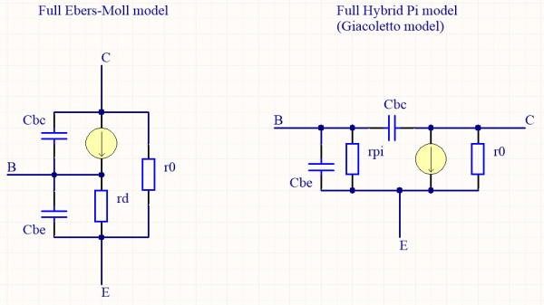
You can easily represent this effect with the same resistance r0 in the Ebers-Moll model ! In fact, there is another imperfection of the transistor which explains some weird structures in circuits : capacitive coupling between base, emitter and collector. Because of their proximity, the poles of a transistor can let some electrons flow even though they shouldn't be able to. This takes form of a capacitor Cbe between base and emitter, and another capacitor Cbc between base and collector. Their value are usually in the picofarad (pF) range, and they limit the amplification effect of a transistor at high frequencies.
There is one last very important thing to note : because small signal analysis only uses small signal variations, constant voltage sources are replaced by ground and constant current sources are replaced by an open connection. This way you don't take into account biasing in small signal analysis, because you should always perform biasing first and it only considers DC sources !
For the sake of completeness, here are the two completed models. They are rarely used, but they can explain some circuit behaviours at high frequency which can be hard to understand otherwise.