About transistors - Part 5 : circuit design and analysis
Today folks, our very first circuit design !
Today folks, our very first circuit design !
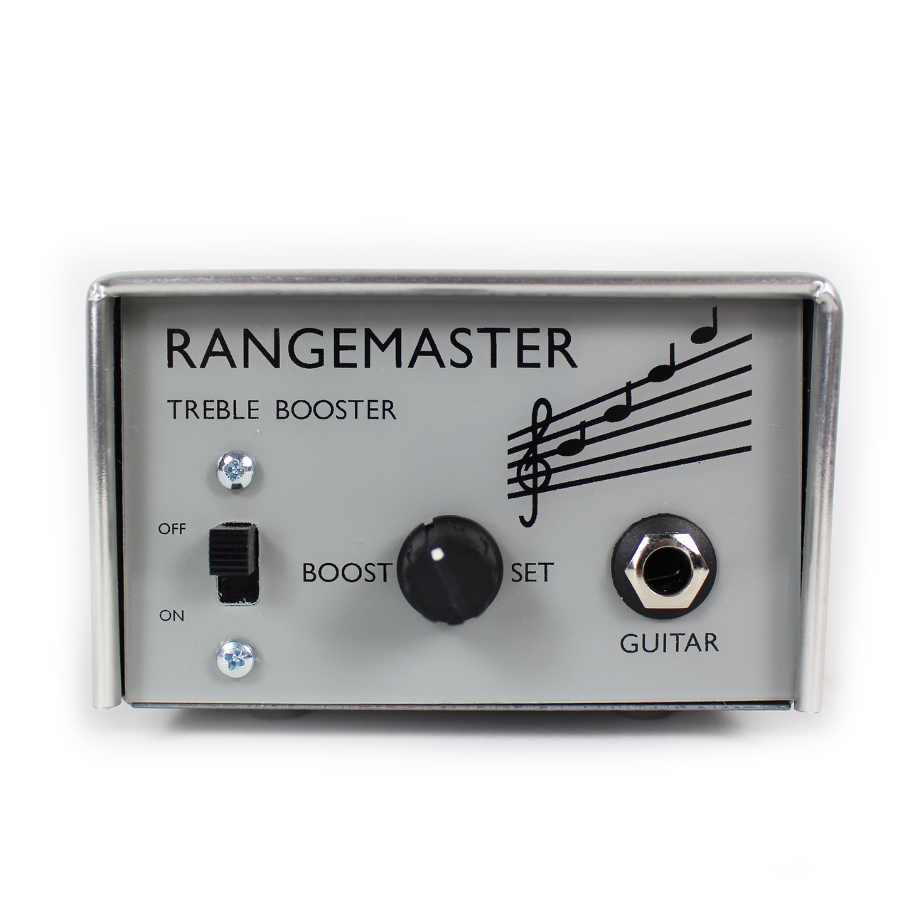
In today’s article we’re gonna design our first transistor circuit ! Two transistors, biasing circuit and some caps will make a good treble booster for guitar use. Both NPN or PNP transistors can be used for that type of booster. For example, the famous and expensive Dallas Rangemaster uses a germanium PNP transistor (OC44). Due to the spread of value accross all parameters, especially the base leakage current, each OC44 needs to be hand selected to improve noise and gain performances. This is the reason why such units cost so much to make and can still be noisier than boosters made of silicon transistors. Electro-Harmonix designed the LPB1 as a simple full range booster using one NPN transistor.
We’d like our booster to be able to drive line inputs and have three different selectable range of boost : full range, high-mid boost, treble boost. Because most electric guitars have a high output impedance, we need our circuit to have a really high input impedance, around 1MΩ. A lower input impedance will cut high frequencies, giving a rounder sound and will be less harsh sounding, so let’s include an option to have a lower input impedance.
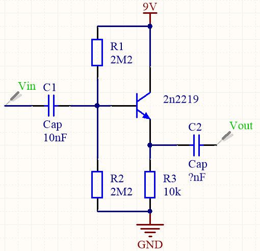
The easiest way to have a high input impedance is to use a buffer circuit. The following circuit uses a 2n2219 silicon transistor and has an input impedance of around 1MΩ. We can show that the input impedance Zin equals to the parallel resistance of R1, R2 and (hfe+1)*R3. The input capacitor removes any DC offset due to the biasing network formed by R1, R2, and forms a high-pass filter with Zin. A value of 10nF for C1 determines a cutoff frequency of 16Hz. The formula giving the frequency of a first order high or low pass filter is the well known f = 1/(2*pi*R*C). However, we do not know the input impedance of the transistor amplifier yet, so we can’t choose a value for C2.
Resistors generate noise depending on temperature and resistance. It is better to use lower values of resistance when possible to improve noise performances. Be careful, as it increases current consumption !
First, we need to determine a resistance at the collector which allows our circuit to drive line level inputs. Our booster could be used as a preamp ! Let’s put a 2.2kΩ pot at the collector (shown as a resistor R6), so we always have a low impedance output. Because DC current flows through this pot however, you may hear scratches when turning it. This configuration is also found in the Dallas Rangemaster and it is in fact the only reason I decided to use it. We’d like to have the maximum output swing available from the transistor, so the collector must stay around 4.5V, which is half of our 9V supply voltage. Ohm’s Law gives us a current of 2mA flowing accross the transistor. DC gain can be used to choose the emitter resistor but because we’re bypassing it with capacitors for full gain, let’s just choose an arbitrary value of 1V at the emitter. This leads to an emitter resistor of 560Ω. If we want to achieve full gain down to 30Hz, we will need a 10uF capacitor in parallel. 420Hz corresponds to a 680nF cap and 1kHz corresponds to a 180nF cap. This way, we only get full gain after the choosen frequency : our full/mid/treble booster is working ! Finally, to bias our transistor correctly, we need a voltage 0.7V higher at the base than the emitter voltage, which is around 1.7V. The resistors R4, R5 forms a voltage divider to bias the transistor around this operating point. The input impedance of the circuit being Zin = R4//R5, we can choose a value for C2 equal to 1uF to let all frequencies enter the booster down to 30Hz. At the output, we need to remove any DC offset and put a load at the output to prevent the cap being left open when nothing is connected. A 100k is a good choice as it won’t interfere with the next impedance too much, and output coupling capacitor C3 has a value of 100nF for a cutoff frequency of 16Hz.
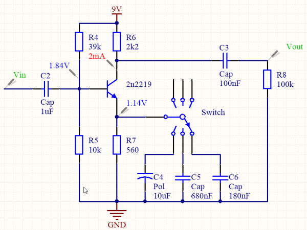
The pot at the collector acts as a load for our transistor in its common emitter configuration. We've seen that the relationship between the current flowing through the transistor and its base-emitter voltage is already dIc = gm*dVbe. Ohm's law gives a corresponding voltage accross the pot equal to dVout = -R6*dIc, hence we get the voltage equation dVout = -gm*R6*dVin. We can calculate gm = 1/R7, hence the voltage gain of the booster : Av = -R6/R7, which is around 4. However, because we are bypassing R7 for high frequencies with our capacitor network, the voltage gain increases a lot until it reaches its maximum value of -R6/rd, around 100 ! This is a selective amplifier.
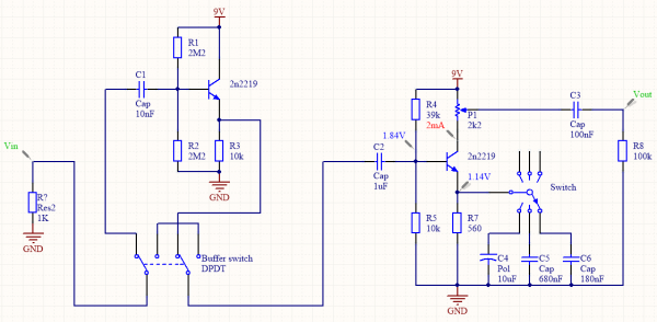
Now we can use a DPDT switch to engage the buffer when we want a full boost, or kill the harsh frequencies when using only the low input impedance booster ! The complete circuit is given in the following picture. The added 1MΩ input resistor gives a reference to the input capacitor to prevent pop when connected to the guitar.
Here, this is as simple as it gets to quickly design a first circuit ! The next step is prototyping, before creating some PCBs and begin production...