About transistors - Part 6 : Advanced circuits
Current mirror, cascode and differential pair !
Current mirror, cascode and differential pair !
Hi everyone ! Welcome to a new episode of About Transistors ! Today, we'll learn about cascode, current mirror and differential pair.
The first circuit I want to explore with you is the cascode amplifier because it introduces the concept of an amplifier bandwidth and active load. An amplifier doesn't boost all the frequencies the same way, we've seen that when designing our guitar treble booster. Because of the parasitic capacitances Cbe and Cbc (see part 4), a common emitter amplifier can only amplify up to a certain frequency, after which the gain of the amplifier decreases. In fact, this is a simple RC network, a low-pass filter with R being the load of the amplifier. However, because of the Miller effect, the capacitance Cbc is multiplied by the gain of the amplifier ! This effect really increases the capacitance from a few picofarads to hundreds of picofarads ! If you have a capacitance C connected between the input and output of a voltage amplifier of gain Av, the capacitance looking from the input is in fact C*(Av+1). We can see now why a high gain amplifier can be severely limited in the high frequencies ! There are some solutions to fight this effect : you can always split the amplification between multiple amplifiers circuits, but you'll need a lot more components and you'll get a lot of noise. The other solution is trying to reduce the load seen from the amplifier. We want to decrease the load R, and the cascode circuit is exactly what we need !
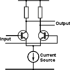
In fact, that's even better : the cascode circuit is made using a common base circuit as an active load for a common emitter configuration. Why does it kill the Miller effect completely ? Well, remember the models for the BJT transistor : the only load for AC seen from the output of the common emitter is the dynamic resistance rd of the common base transistor. Which is well below 1k. Hence we can now drive a really higher load while maintaining a high bandwidth. This configuration isn't really useful "as is" in audio amplifiers, because the bandwidth in audio is pretty narrow - 20 Hz to 20 kHz. However it is widely used in radiofrequency amplifiers, and existed well before transistors where invented. Yes, that's true, cascode amplifiers had the same function with tubes, and it also exists for FET transistors ! The following picture shows a cascode circuit and its equivalent circuit model for small signals. The gain of the circuit is the same as for the common emitter amplifier, but it has an increased bandwidth and is immune to the Miller effect. dVout = gm*Load*dVin.
%20-%20Sheet1.SchDoc%20_%20-%20Mid%20booster.PrjPcb.%20Not%20signed%20in..png?1567459898422)
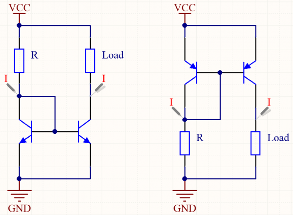
Let's talk about another well-known circuit in analog electronics : the current mirror. An advanced structure meant to copy and paste a current wherever you need it ! It uses two transistors which should theoretically be exactly matched to work well. The circuit is actually pretty simple. Because a transistor is only controlled by its base-emitter voltage, having two exact same transistors with a common base terminal should lead to the same current flowing in them. And it works pretty well ! We know that, at DC, Vbe is approximately equal to Vd, hence we the current flowing through the resistor R in the circuit is I = (VCC-Vd)/R, and it is the same current in both transistors. The picture shows both the NPN and PNP versions of this circuit. NPN version is sometimes named current sink, PNP version being current source. You can also tie multiple transistors to the base of the first one, to control multiple current branches. However, please remind that a BJT transistor takes a little bit of current in its base, even though we often don't take it into account ! Too much transistors will make the voltage fall at the base and the current will decrease.
The last circuit I want to talk about is the differential pair, also called long-tailed pair because of the resistor common to both branches. This is a special type of amplifier, a differential amplifier, meaning it amplifies the difference of voltage between its two inputs. By grounding one input, you can use it for amplifying a simple signal, and you can choose to have one or two outputs to make it single-ended or fully differential. If V1 is higher than V2, then the current increases if Q1. Because we want the current in the emitter resistor to stay constant, it means we have a decreasing current through Q2 in the same quantity. Hence the voltage at VC2 is higher than at VC1. This structure is in fact a double common-emitter configuration, and it is also inverting. We can show with a few maths that dVc1 - dVc2 = gm*R*(dV1 - dV2), with gm being negative and R the collector load resistors. However in practice, the current in the emitter resistor varies with voltage, making this circuit not as stable as we want it to be. The answer is an active load. Let's put a NPN transistor instead of the resistor and bias it so we have the same current (circ. 2). This time, the current does not vary as much when operating !
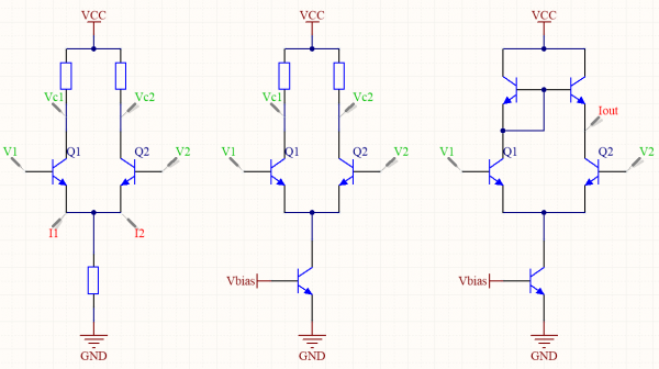
The last variation is slightly intriguing and I have never seen one website really explaining how it works. Strangely, that's a fundamental circuit to design operationnal amplifiers and there are just too much circuits using it for me not to talk about it. In this version, we really want the exact same current through both branches to have perfect symetry in operation. Doing so dramastically improves the common-mode rejection ratio. This number with a weird name is just the ability of our circuit to make a perfect difference. If branches current are not the same, the output also gets a little bit of the sum of the input instead of the difference only : VOUT = Adiff*VDIFF + Asum*VSUM. Of course, we want the differential gain Adiff as high as possible and the common-mode gain Asum as low as possible for the best behaviour of this circuit. The common-mode rejection ratio is CMRR = Adiff/Asum. The solution lies in this article : let's use a current mirror ! This way, no current will be able to vary in the collector load of both transistors. When we apply a voltage difference between the input of the circuits, where does the current go ? Well, into the load ! We have built a differential transconductance amplifier, which outputs current for a given input voltage. Trust me, this is really useful, because there is now one last question we need to answer. What happens if we put a voltage amplifier right after this circuit ? Well, because the input impedance of the voltage amplifier is theoretically infinite, we get... infinite gain ! In practice the limiting factor for gain is the Early resistors of the current mirror. Then the voltage gain of the circuit is Adiff = gm*(r0//Zin) with Zin the input impedance of the following circuit.
That's all - and a lot ! - for this article. Take the time to go back or skip if you don't understand everything at once ! See you later !